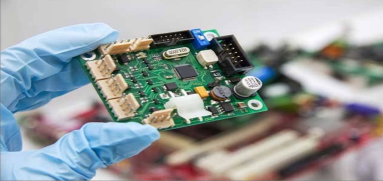


Low volume PCB assembly
The manufacture and fabrication of printed circuit boards (PCBs) is a complex procedure that includes stages like design, production, and verification. As most of the forming operation is now computerized, these PCBs may be manufactured in bulk or in low quantities as necessary. Prototype production is simply which low volume PCB assembly entails. The low frequency assembly procedure like normal production, consists of three basic steps: fabrication, element positioning, as well as assembly
What is Low Volume PCB Assembly?
The technique of attaching parts to a smaller number of blank PCBs is known as low volume PCB assembly. The count of chips in such a set is as within about 250 or as much as fewer than that. Because of the smaller batch sizes, this technique is also known as small-volume manufacturing. The cost of PCB assembly also depends on procedure.
Depending on scale factor, whether minor or big, the reliability of a panel is dependent on the agreement company's as well as the hardware's synchronisation of a DFM and DFA processes. Such limited assembly is suitable for complicated or unique PCBs.
Low Volume PCB Assembly is used for prototype and system development
PCBs utilized in medicinal, aviation, government and defence, mobile communications, and other industries have intricate structures. Also with smart element placement, PCB assembly necessitates a continuous development process. Prototyping refers to the testing or repeat method of PCB construction. Prototyping is a stage before large scale production that allows electrical OEMs as well as development directors to explore with various ideas. A low output PCB assembly method has been shown to provide a solid basis for PCB development. It provides both continuous and sequence prototyping, as well as careful analysis of product design, design for chamber and design for functioning.
Here are the prototype possibilities and their connectivity to DFM, DFA, and DFT on the UETPCB website.
Sequential PCB Prototype: In this kind of prototyping, a simple modification is integrated on many panels for each process, while subsequently the entire process is evaluated for performance. In addition, the element attachment pattern are sometimes modified on different panels of various characteristics, and the similar modification can be tested with different outcomes. This technique, that is DFT, is appropriate for efficient checking.
Parallel PCB Prototyping: Separate modifications are performed on different panels. All of these modifications are being evaluated for performance. For instance, one pcb may be made of a special composition than another, and each may have a distinct circuit arrangement. This technique, which is DFA, is useful for testing different designs.
Elements affecting limited capacity PCB assembly prototyping:
- These preceding are a few significant characteristics that contribute to the effectiveness of limited design using Material selection, DFA, and DFT.
- This is simple to maintain track of acceptable components that must utilise, controller schematics, and so on throughout a limited industrial phase. It improves efficiency of the production cycle
- The dose not put (DNP) methodology provided through low margin prototype is appropriate for the optimum organization for verification (DFT). DNP limits part location, which can cause monitoring and coding hard.
- Because it allows easy requirements gathering below various conditions, development changes are quick with this method. The more significant amount of model cycles is an opportunity for such an expert to pick an effective system.